| P/N
|
Q28-100G3934-BX40/Q28-100G3439-BX40
|
Vendor Name
|
OEM
|
| Form Factor
|
QSFP28
|
Max Data Rate
|
111.8Gbps
|
| Wavelength
|
TX1309nm/RX1304nm
|
Max Distance
|
40km
|
| Connector
|
Simplex LC
|
Transmitter Type
|
EML
|
| Cable Type
|
SMF
|
Receiver Type
|
APD
|
| DDM Support
|
Yes
|
Modulation Format
|
PAM4
|
| TX Power
|
1.7~+7.1dBm
|
Receiver Sensitivity
|
< -13.8dBm
|
| Protocols
|
802.3cu, SFF-8636 & SFF-8679,
100G OTU4, QSFP28 MSA
|
Operation Temperature
|
0 to 70°C (32 to 158°F)
|
Absolute Maximum Ratings
|
Parameter
|
Symbol
|
Min
|
Typical
|
Max
|
Units
|
Notes
|
|
Storage Temperature
|
TS
|
-40
|
|
+85
|
degC
|
|
|
Supply Voltage
|
VCC
|
-0.5
|
-
|
+4.0
|
V
|
|
|
Operating Relative Humidity
|
RH
|
-
|
-
|
+85
|
%
|
|
Recommended Operating Environment
|
Parameter
|
Symbol
|
Min
|
Typical
|
Max
|
Units
|
Notes
|
|
Operating Case Temperature
|
Tc
|
0
|
|
70
|
°C
|
|
|
Power Supply Voltage
|
VCC
|
3.13
|
3.3
|
3.47
|
V
|
|
|
Power Supply Current
|
ICC
|
-
|
-
|
1.3
|
A
|
|
|
Maximum Power Dissipation
|
PD
|
-
|
-
|
4.5
|
W
|
|
|
Data Rate(optical)
|
DRo
|
-
|
106.25
|
-
|
Gb/s
|
|
|
Transmission Distance
|
TD
|
-
|
-
|
40
|
km
|
Over SMF
|
Optical Characteristics
|
Transmitter
|
|
Parameter
|
Symbol
|
Min.
|
Typical
|
Max.
|
Unit
|
Notes
|
|
Center Wavelength
|
Q28-100G3439-BX40
|
CW
|
1303.54
|
1304.58
|
1305.63
|
nm
|
|
|
Q28-100G3934-BX40
|
CW
|
1308.09
|
1309.14
|
1310.19
|
|
|
|
Average Launch Power
|
PTX
|
1.7
|
-
|
7.1
|
dBm
|
1
|
|
Outer Optical Modulation Amplitude
|
OMA
|
4.5
|
-
|
7.9
|
dBm
|
TEDCQ<1.4
|
|
3.3+TDECQ
|
-
|
dBm
|
TEDCQ>1.4
|
|
Transmitter and dispersion eye closure for PAM4 (TDECQ) (max)
|
TDECQ
|
-
|
-
|
3.9
|
dBm
|
|
|
|TDECQ-TECQ| (max)
|
-
|
-
|
-
|
2.7
|
dB
|
|
|
Average Output Power (Laser Turn off)
|
P0UT-OFF
|
-
|
-
|
-15
|
dBm
|
|
|
Side Mode Suppression Ratio
|
SMSR
|
30
|
-
|
-
|
dB
|
|
|
Extinction Ratio
|
ER
|
6
|
-
|
-
|
dB
|
|
|
Receiver
|
|
Center Wavelength
|
Q28-100G3439-BX40
|
CW
|
1308.09
|
1309.14
|
1310.19
|
nm
|
|
|
Q28-100G3934-BX40
|
1303.54
|
1304.58
|
1305.63
|
|
|
|
Damage threshold
|
Pdamage
|
-2.4
|
-
|
-
|
dBm
|
2
|
|
Average Rx Power
|
PRX
|
-16.0
|
-
|
-3.4
|
dBm
|
3
|
|
Receive power_OMAouter
|
POMA
|
-
|
-
|
-2.6
|
dBm
|
|
|
Receiver sensitivity _OMAouter
|
SEN _OMA
|
-
|
-
|
-13.8
|
dBm
|
4
|
|
Los Assert
|
LosA
|
-26
|
-
|
-
|
dBm
|
|
|
Los De-Assert
|
LosDA
|
-
|
-
|
-15
|
dBm
|
|
|
Los Hysteresis
|
LosH
|
0.5
|
-
|
-
|
dB
|
|
Notes:
1. The optical power is launched into SMF.
2. The receiver shall be able to tolerate, without damage, continuous exposure to an optical input signal having this average power level. The receiver does not have to operate correctly at this input power.
3. Average receive power, each lane (min) is informative and not the principal indicator of signal strength.
4. Measured with conformance test signal at TP3 using the test pattern PRBS31Q or scrambled idle for stressed receiver sensitivity for the BER= 2.4x10⁻⁴.
Electrical Characteristics
|
Transmitter (Module Input)
|
|
Parameter
|
Symbol
|
Min.
|
Typical
|
Max.
|
Unit
|
Notes
|
|
Input Differential Impedance
|
Rin
|
-
|
100
|
-
|
Ohm
|
|
|
Differential Data Input Amplitude
|
VIN,P-P
|
80
|
-
|
900
|
mVpp
|
|
|
Differential termination mismatch(max)
|
D-mismatch
|
-
|
-
|
10
|
%
|
|
|
DC common-mode input voltage
|
|
-0.3
|
-
|
2.8
|
V
|
|
|
Transition time (20%~80%)
|
TrTf
|
10
|
-
|
-
|
ps
|
|
|
LPMode, Reset and ModSelL/Txdis
|
VIL
|
-0.3
|
-
|
0.8
|
V
|
|
|
LPMode, Reset and ModSelL/Txdis
|
VIH
|
2.0
|
-
|
VCC+0.3
|
V
|
|
|
Receiver (Module Output)
|
|
Output Differential Impedance
|
Rout
|
-
|
100
|
-
|
Ohm
|
|
|
Differential Data Output Amplitude
|
VOUT.P-P
|
-
|
-
|
900
|
mVpp
|
|
|
Differential termination mismatch(max)
|
D-mismatch
|
-
|
-
|
10
|
%
|
|
|
Transition time, 20%to80%
|
TrTf
|
12
|
-
|
|
ps
|
|
|
ModPrsL and IntL/ Rx los
|
VOL
|
0
|
-
|
0.4
|
V
|
|
|
ModPrsL and IntL/ Rx los
|
VOH
|
VCC-0.5
|
-
|
VCC+0.3
|
V
|
|
Digital Diagnostics
|
Parameter
|
Range
|
Accuracy
|
Unit
|
Calibration
|
|
Temperature
|
0 to 70
|
±3
|
oC
|
Internal
|
|
Voltage
|
0 to VCC
|
0.1
|
V
|
Internal
|
|
Tx Bias Current
|
0 to 100
|
10%
|
mA
|
Internal
|
|
Tx Output Power
|
1.7 to 7.1
|
±3
|
dBm
|
Internal
|
|
Rx Power
|
-16.0 to -3.4
|
±3
|
dBm
|
Internal
|
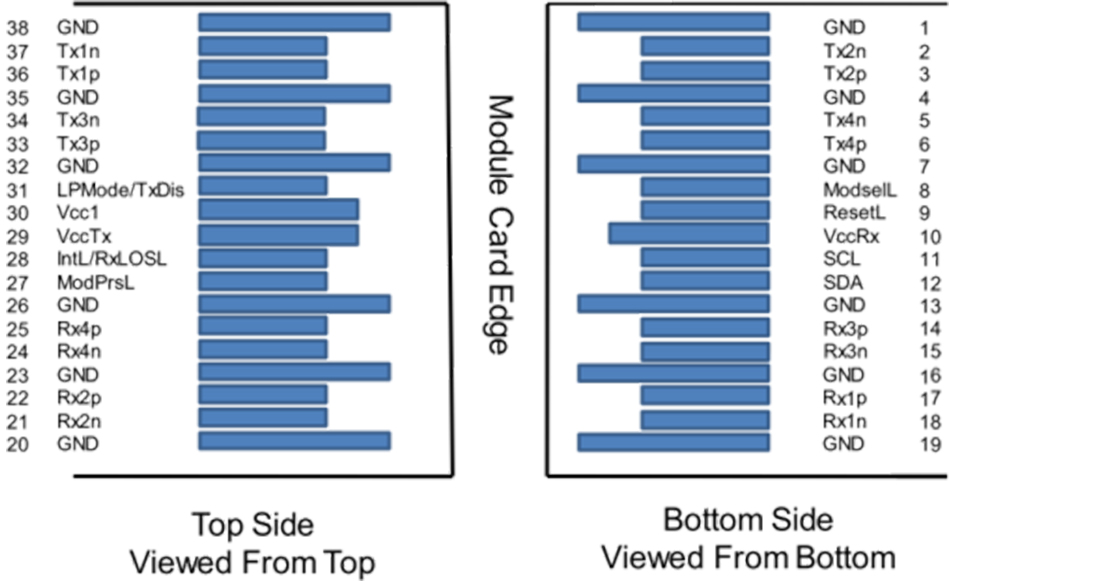
Pin Assignment

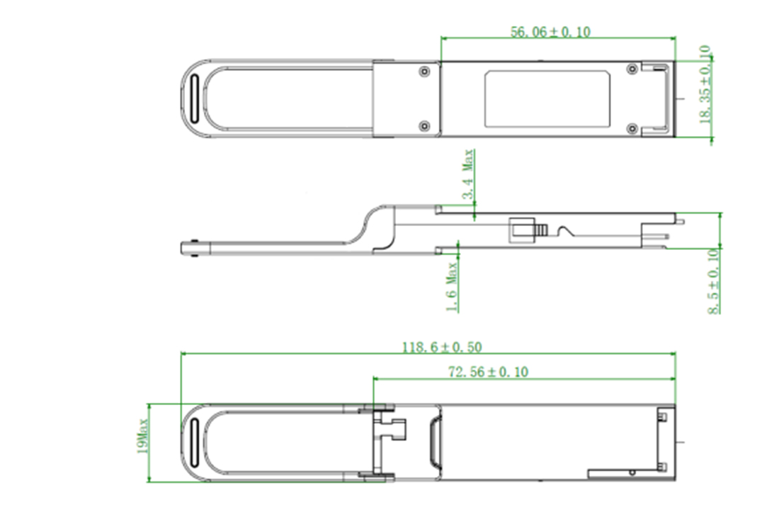
Mechanical Dimension


